A potential changing bipolar junction transistor for thermoelectric applications
Received: 27-Apr-2023, Manuscript No. PULJPAM-23-6388; Editor assigned: 29-Apr-2023, Pre QC No. PULJPAM-23-6388 (PQ); Reviewed: 13-May-2023 QC No. PULJPAM-23-6388; Revised: 27-Aug-2023, Manuscript No. PULJPAM-23-6388 (R); Published: 04-Sep-2023, DOI: 10.37532/2752-8081.23.7(6).1-2.
Citation: Lu X, Liang Q, Liang Y . A potential changing bipolar junction transistor for thermoelectric applications. J Pure Appl Math 2023;7(6):1-2.
This open-access article is distributed under the terms of the Creative Commons Attribution Non-Commercial License (CC BY-NC) (http://creativecommons.org/licenses/by-nc/4.0/), which permits reuse, distribution and reproduction of the article, provided that the original work is properly cited and the reuse is restricted to noncommercial purposes. For commercial reuse, contact reprints@pulsus.com
Introduction
A novel potential‐changing bipolar junction transistor is designed where collector‐base junction has a larger barrier potential than emitter‐base junction. As carriers move from the emitter to the collector, they experience a potential rise and absorb heat due to Peltier effect in semiconductors. Such kind of transistor can be used for refrigeration and solar electricity with high efficiency.
Description
A barrier potential exists in the P‐N junction of semiconductors. When carriers move from the P‐region to the N‐region, they experience a potential drop and heat extraction, or an increase in potential and heat absorption when moving from the N‐region to the P‐region. However, the conventional thermoelectric diodes have very low efficiency.
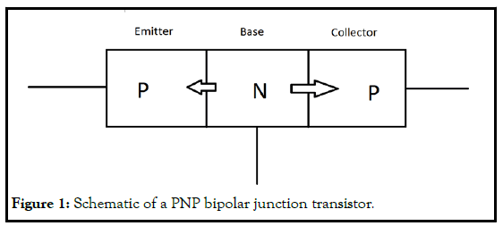
In this work, we designed a thermoelectric Bipolar Junction Transistor (BJT) which has three terminals instead of two terminals in a diode. There are two P‐N junctions in a BJT. They are emitter‐base junction and collector‐base junction. The two junctions have opposite field directions. The emitter‐base junction has a small barrier potential while the collector‐base junction has a large barrier potential. The emitter‐base is forward biased, and the collector is connected to the load without bias. A schematic of PNP transistor is shown in Figure 1. As indicated by the arrows, the collector‐base junction has a larger barrier potential than the emitter‐base junction.
When carriers move from the emitter to the base, most of them are swept to the collector due to the collector‐base junction field. The total potential change is equal to the sum of potentials which is actually the subtraction of the two barriers due to their opposite directions. If the barrier potentials are significantly different, the total potential change is not zero. For example, silicon‐graphene and germanium‐graphene have junction barriers of 0.64 eV and 0.22 eV, respectively. BJT can be made of germanium‐graphenesilicon, which serve as emitter, base and collector respectively. The potential change per carrier passing through the transistor is 0.42 eV. If the collector is made of SiC, or GaN, the potential change would be much higher. The carriers will absorb heat corresponding to the potential rise due to the Peltier effect in semiconductors. The current through base is negligible because it only counts ~2% of the total current.
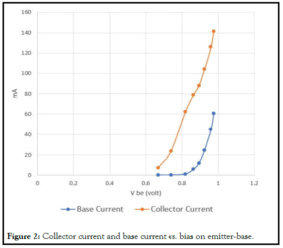
Could current flow to the collector which is not biased? The answer is YES. We measured the collector current as well as the base current of 2N3906, which is a PNP transistor. The emitter‐base is forward biased, while collector‐base is unbiased connected to a 10 ohm load. The data is shown in Figure 2. However, 2N3906 is not a potential‐changing transistor yet because its two junctions have similar barrier potentials.
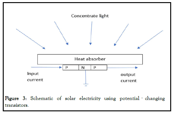
Potential‐changing transistor is a good candidate for solar electricity. Figure 3 shows the schematic of solar electricity. A heat absorber collects heat from the concentrated sun light and its back is attached to an array of potentialchanging transistors.
Conclusion
The transistor generates power whenever its potential difference is maintained by the solar heat. The efficiency is expected to be higher than a solar panel.


