


Derivation of Digital-to-Analog Converter Architectures Based on Number Theory
Received: 14-Oct-2022, Manuscript No. puljpam- 22-5518; Editor assigned: 16-Oct-2022, Pre QC No. puljpam- 22-5518 (PQ); Accepted Date: Oct 26, 2022; Reviewed: 20-Oct-2022 QC No. puljpam- 22-5518 (Q); Revised: 21-Oct-2022, Manuscript No. puljpam- 22-5518 (R); Published: 30-Oct-2022, DOI: 10.37532/2752-8081.22.6(5).14-24.
Citation: Bai X, Yao D, Du Y, et al. Derivation of Digital-to-Analog Converter Architectures Based on Number Theory. J Pure Appl Math. 2022; 6(5):14-24.
This open-access article is distributed under the terms of the Creative Commons Attribution Non-Commercial License (CC BY-NC) (http://creativecommons.org/licenses/by-nc/4.0/), which permits reuse, distribution and reproduction of the article, provided that the original work is properly cited and the reuse is restricted to noncommercial purposes. For commercial reuse, contact reprints@pulsus.com
Abstract
This paper investigates possibilities of deriving new Digitalt toAnalog Converter (DAC) architectures based on polygonal and prime number theories. As the result, configurations of polygonal number DACs and prime number DACs are obtained; each consists of a few current sources, a resistor network, switch arrays and a decoder circuit. Whole circuits are designed and their operations are confirmed with simulation; they work as DAC in principle, and most of their circuits consist of digital circuit, which is suitable for implementation with nano-CMOS process. In many cases, analog/mixed-signal circuit architecture design relies on intuitions and experiences of the designer, but here we demonstrate that it is feasible to derive different DAC architectures from conventional ones based on mathematical theory.
Keywords
Digital-to-analog converter; DAC; Number theory; Polygonal number; Prime number
Introduction
Analog /mixed-signal circuit design is art rather than technology, with which industry can differentiate their electronic products. There Analog-to-Digital Converters (ADCs) and Digital-to-Analog Converters (DACs) are especially important [1-4]. Their design mostly relies on intuitions and experiences of mature designers, rather than mathematical theory; only one exception is analog filter synthesis and analysis [5]. On the contrary, the authors have been involved in the research for applications of classical mathematics - such as number theory to their design; in this viewpoint, our research results have been reviewed and summarized in [6-13]. This paper introduces new DAC architecture derivation from number theory to validate our argument that classical mathematics can explore new analog and mixed-signal circuit design. The derived DAC architectures may not well incorporate circuit non-ideality effects such as device mismatches. However, this attempt may lead to new DAC architecture derivation methodology, and this paper shows its first step.
Our previous research results for applications of classical mathematics to analog/mixed-signal circuit designs are summarized as follows.
Fibonacci sequence weight SAR ADC
We have investigated SAR ADC design using a redundant SAR search algorithm with Fibonacci sequence weight. We showed that this method can realize high speed SAR AD conversion when the internal DAC incomplete settling is considered [14].
Metallic ratio sampling
We have investigated efficient waveform acquisition conditions between the measured waveform repetitive frequency (fsig) and the sampling clock frequency (fCLK) in an equivalent-time sampling system, when the measured waveform is periodic. We have obtained that in case that fCLK/fsig is a metallic ratio, waveform missing phenomena for the equivalent-time sampling can be avoided and highly efficient waveform acquisition sampling can be realized [15-17]. This technique can be used for analog/mixed-signal IC testing where the input signal is controllable.
Residue sampling
We have investigated the residue sampling circuit which provides high-frequency signal estimation using multiple low-frequency sampling circuits following an analog Hilbert filter and ADCs; the sampling frequencies are relatively prime. It is based on aliasing phenomena in the frequency domain for waveform sampling and the residue number theory [18, 19].
Efficient ADC histogram testing condition
We have studied the ADC testing efficiency improvement of the histogram method by investigating the ratio between the input frequency and the sampling frequency to shorten ADC test time, and we have found that the metallic ratio is effective [20].
Non-uniform current division resistive DAC
We have studied design and analysis of DACs based on the non-uniform current division resistive ladder, and proposed a new configuration DAC with segmentation of binary, quaternary and unary resistive-ladders, which enables two times gain with equivalent chip area and current sources to the conventional one [21-23].
Gray code input DAC
We have also investigated three types of Gray-code input DAC architectures (current-steering, charge-mode and voltage-mode DACs) for glitch reduction and hence clean signal can be generated [24, 25].
2D Layout of unit cells with pseudo random selection order for unary DAC
We have investigated pseudo random selection order algorithms for the segmented DAC linearity improvement, by cancelling systematic mismatch effects among unit cells [26-29]. We consider their 2D array layout with systematic errors. If they are laid out and selected in a regular manner, the systematic errors are accumulated at the DAC output, which causes large non-linearity. If they are selected pseudo-randomly, they can be cancelled to some extent. The investigated pseudo-random selection algorithms are based on Magic Square, Latin Square as well as Euler’s Knight Tour.
Polygonal number DAC and prime number DAC
We have proposed the preliminary ideas of the following DAC configurations based on number theory (i) The DAC consists of N current sources, N switch arrays, an N-polygonal number weighted resistor network, and a decoder (N= 3, 4, 5, ...); this is based on the polygonal number theory [30-32]. (ii) The DAC consists of 2 current sources, 2 switch arrays, a prime number weighted resistor network, and a decoder (N= 3, 4, 5, ...); this is based on the Goldbach conjecture. This paper discusses the derivation of these DACs from the number theory in details. This paper shows that the derivation of very new DAC configurations from the number theory is possible, and demonstrates their operations in principle as the first step. Also the possibility of dynamic element matching (DEM) technique usage to take care of the device mismatch effects is described [3, 12].
The outline of this paper is as follows: Section 2 shows the derivation of the polygonal number DAC from the polygonal number theorem and its configuration as well as operation verification with simulation. Section 3 shows the derivation of the prime number DAC from Goldbach conjecture and its configuration as well as operation with simulation. Section 4 provides conclusion.
Polygonal Number DAC
This section describes derivation of our polygonal number DACs.
Polygonal number theory
This subsection briefly explains polygonal numbers in number theory. We take the triangular number as an example, and infer that this consideration can also applicable to other polygonal numbers through the simulation results of the triangular number.
Polygonal numbers are represented as dots or pebbles arranged in the shape of a regular polygon; they are triangular numbers, square numbers, pentagonal numbers, hexagonal numbers, heptagonal numbers, octagonal numbers, and so on, as shown in Figure 1.

Figure 1: Explanation of polygonal numbers. (a) Triangular numbers (b)Square numbers. (c) Hexagonal numbers
For example, the triangular numbers are given by as follows (see Figure. 1 (a)):1, 3, 6, 10, 15, 21, 28, 36, 45, 55, 66, 78, 91, 105…, n(n+1)/2, …
We design DACs based on the following triangular number theoretical properties.
Triangular number theorem:
“Any natural number is composed of 3 or less than 3 triangular numbers”. Figure. 2 shows its explanation.

Figure 2: Explanation of triangular number theorem.
Triangular number DAC
Our derived DAC based on the triangular number theorem is shown in Figure. 3. It consists of 3 current sources, 3 switch arrays, a triangular number weighted resistor network and a decoder circuit.

Figure 3: Proposed triangular number DAC.
Triangular number weighted resistor network
First, we consider the resistor network in Figure. 4 (a) and we obtain the output voltage VOUT as follows:
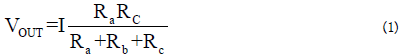

Figure 4: Basic resistor networks. (a) Three resistors with an input current source. (b) Extension to K resistors and a load resistor Rc
Here Rc is a load resistor and we see that it changes the gain of the resistive network. Its extension to the network of K resistors and a load resistor Rc is shown in Figure. 4 (b).
The key component of the triangular number DAC is the triangular number weighted resistor network in Figure. 5, where Rn in Figure. 4 (b) is replaced with n R (n=1, 2,…, K) and R is a unit resistor.

Figure 5: Triangular number weighted resistor network.
Figure. 6 shows the triangular number weighted resistor network with K=5 and an input current source applied to each node.
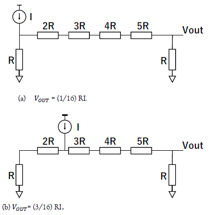
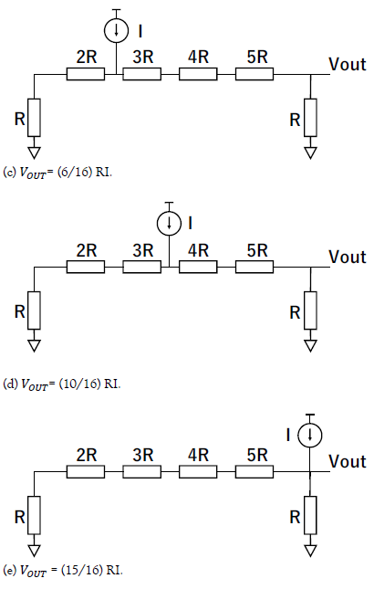
Figure 6:Operation of the triangular number weighted resistor network, which generates a triangular number weighted voltage at VOUT .
We have the following from Figure. 4 (a) and Eq. (1):

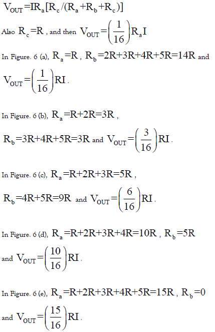
Notice that 1, 3, 6, 10, 15 are triangular numbers.
We see that the triangular number weighted resistor network generates a triangular number weighted voltage at VOUT when a current is injected to one node.
We have performed SPICE simulation for the circuits in Figure. 7. Simulation circuit is shown in Figure. 7 (a), where R = 1kΩ. The waveforms of the input current sources I1 ~I5 are shown in Figure. 7 (b) and the waveform of Vout is shown in Figure. 7 (c); we see that this simulation result confirms the operations of the circuits in Figure. 6, with R = 1kΩ and I = 100μA.
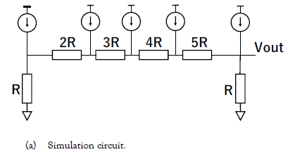
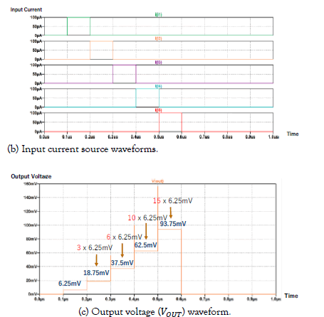
Figure 7: SPICE simulation of the proposed triangular number weighted resistor network.
Three current sources and three switch arrays
Based on the theoretical properties of the triangular numbers and the superposition principle, we obtain the input combination for the digital input from 0 to 30 by controlling three switch arrays for three current sources, according to Figure. 2. The output of the three current sources is the superposition of the output results of a single current source, so we obtain the results as shown in Figure. 7. For example, in the case of the input 9, we need to input two current sources, that is, superimposition of Figure. 6 (b) and Figure. 6 (c) becomes Figure. 8 (a).
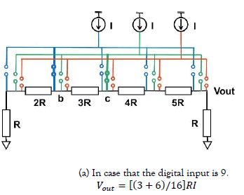
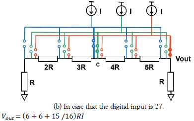
Figure 8: Superposition of three current sources to the investigated triangular number weighted resistor network.
Decoder design
We have designed a decoder logic for a 6-bit triangular number DAC. Its digital inputs are from 0 to 63, and three switch arrays corresponding to three current sources is represented by Sa, Sb and Sc respectively. There are 11 switches in the switch array of each current source, which are represented by Sa00... Sa10, Sb00... Sb10, Sc00... Sc10.
Due to the large number, we cannot verify the assumptions one by one, so we write an automatic verification program to detect whether all the input conditions are in line with our conjecture. The following is the design principle of the verification program:
Suppose that the digital input is 5 in decimal or B5, B4, B3, B2, B1 and B0 are 000101 in binary. Notice that 1+1+3=5 as shown in Figure. 2. Then three switches of Sa1, Sb1, and Sc2 are ON (Sa1 =1, Sb1 = 1, Sc2 = 1) and the other switches are OFF, as shown in Figures. 9, 10.

Figure 9: DAC decoder logic for the digital input of 5.

Figure 10: Three current sources connection to the triangular number weighted network for the digital input of 5.
The triangular number DAC decoder has the digital inputs of B5, B4, B3, B2, B1, B0 (from 0 to 63 in decimal) and the digital outputs of Sa00, Sa01, Sa02, … Sa10, Sb00, …Sb10, Sc00, … Sc10. Each output logical expression from B5, B4, B3, B2, B1, B0 can be obtained from Fig. 2, and each logical expression is verified by a C program with the following algorithm:
Data A, Data B, Data C and Data are defined as follows:
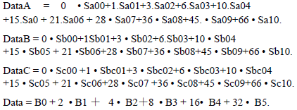
Here Sa00, Sa01, Sa02, … Sa10, Sb00, …Sb10, Sc00, … Sc10 are written as designed decoder logical expressions of B5, B4, B3, B2, B1, B0.
The program ran from B5 B4 B3 B2 B1 B0 = 000000 to 11111 and verified the following in all cases:
If Data = DataA + DataB + DataC, the output is OK. If Data ! = DataA + DataB + DataC, the output is WRONG.
When for all B5, B4, B3, B2, B1, B0, the output is OK, then the decoder logical expressions are correct. The verification program execution results are as shown as Figure. 11.

Figure 11: Execution result of the triangular number DAC decoder verification program.
Remark 1
According to the triangular number theory, any natural number is the sum of three, two or one of triangular numbers. However, notice that its expression is not unique; a given natural number n can be represented by n = n1+ n2+n3and n = m1+m2 + m3where n1, n2,n3, m1,m2 and m3 are triangular numbers or 0. For example, in case n=29, 25=10+15 and 25=1+3+21. For the decoder design, we choose one of them for a given input data.
General polygonal number dac
In general, N-polygonal number theorem is given as follows (N=3, 4, 5, 6, …):
The polygonal number theory:
“Any natural number is composed of N or less than N-polygonal numbers.”
This polygonal number theorem was conjectured by French mathematician, Pierre de Fermat and proved by French mathematician, Augustin-Louis Cauchy.
Figure. 12 shows out proposed DAC configuration using N-polygonal number properties, which is composed of N current sources, N switch arrays, an N-polygonal number weighted resistor network and a decoder circuit; these are based on the above polygonal number theorem.

Figure 12: DAC configuration based on N-polygonal number
N-Polygonal Number Weighted Resistor Network
Now we will explain N-polygonal number weighted resistor networks.
The n-th N-polygonal number PN (n) is given as follows:
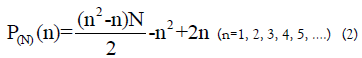
or 1, N, 3N-3, 6N-8, 10N-15, ….
Then the N-polygonal number resistor network using Figure. 4 (b) is designed as follows:
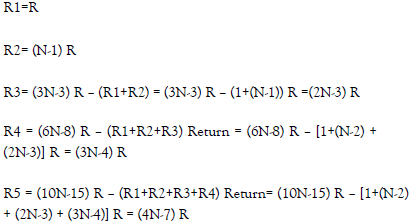
Figure. 13 shows the N-polygonal number weighted resistor network with K=5 and an input current source is applied to each node.
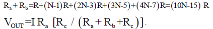
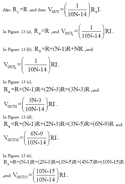

Figure 13: Designed N-polygonal number weighted resistor network.
Notice that 1, N, 3N-3, 6N-9, 10N-15 are N-polygonal numbers. They are 1, 3, 6, 9, 15 for N=3 and they are 1, 4, 9, 25, 36 for N=4, while they are 1, 6, 15, 27, 45 for N=6.
We see that the N-polygonal number weighted resistor network generates an N-polygonal number weighted voltage at Vout when a current is injected to one node.
Prime Number DAC
This section describes derivation of our prime number DACs.
Prime number theory
Prime number is a natural number greater than 1 that cannot be formed by multiplying two smaller natural numbers.
Prime numbers:2, 3, 5, 7, 11, 13, 17, 19, 23, 29,…..
Goldbach conjecture is given as follows (Figure. 14):

Figure 14: Explanation of Goldbach conjecture.
“All even numbers can be represented by the sum of two prime numbers.”
The above conjecture has not been proved yet. However, we can check with numerical calculation that the above conjecture is valid, for example, up-to 221 for 20-bit DAC design.
Prime number DAC
Figure. 15 shows our proposed prime number DAC circuit based on Goldbach conjecture, which consists of 2 current sources, 2 switch arrays, a prime number weighted resistor network and a decoder circuit.

Figure 15: Proposed prime number DAC.
We consider the mapping from even number obtained by addition of two prime numbers to the DAC digital input, as shown in Figure. 16. Then we have the digital input by “divide by 2 (1-bit right shift)” of two-prime-number addition.

Figure 16: Mapping from even number obtained by addition of two prime numbers to digital input.
Prime number weighted resistor network
Figure. 17 shows the prime number weighted resistor network and an input current source applied to each node. Here
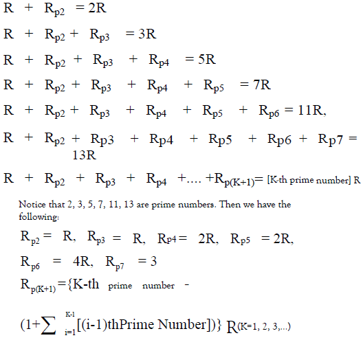

Figure 17: Designed prime number weighted resistor network.
We have the following in Figure. 18 from Figure. 4 (a) and Eq. (1):
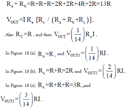
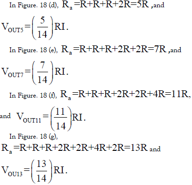
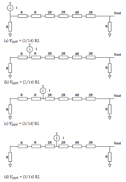
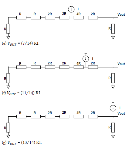
Figure 18: Operation of the prime number weighted resistor network, which generates the prime number weighted voltage.
Figure. 19 (a) shows the case that the digital input is 6 while Figure. 19 (b) is the case it is 8.
Figure 19: Prime number DAC operation
Note that 5+7 = 2x6 and 5+11 = 2x8. Figure. 20 shows the SPICE simulation verification.
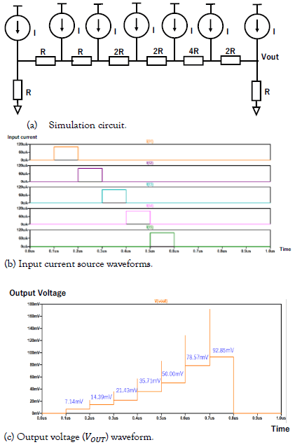
Figure 20: SPICE simulation of the proposed prime number weighted resistor network.
Switch arrays and decoder design
We have also designed a decoder logic for a prime number DAC. Its digital inputs are from 0 to 63, and two switch arrays corresponding to two current sources is represented by Sa and Sb. There are 23 switches in the switch array of each current source, which are represented by Sa00... Sa22, Sb00... Sb22.
Due to the large number, we cannot verify the assumptions one by one, so we write an automatic verification program to detect whether all the input conditions are in line with our conjecture. The following is the design principle of calibration program:
Suppose that the digital input is 10 in decimal or B5, B4, B3, B2, B1 and B0 are 000101 in binary. Notice that 3+7=10 as shown in Figure. 19. Then three switches of Sa1 and Sb1 are ON (Sa3 =3, Sb5 = 7) and the other switches are OFF, as shown in Figures. 21, 22.
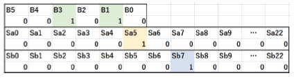
Figure 21: DAC decoder logic for the digital input of 10.
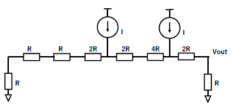
Figure 22: Two current sources connection to the prime number weighted network for digital input of 10.
The prime number DAC decoder has the digital inputs of B5, B4, B3, B2, B1, B0 (from 0 to 63) and the digital outputs of Sa00, Sa01, Sa02, … Sa22, Sb00, …Sb22. Each logical expression is verified by a C program with the following algorithm:
Data A, Data B, and Data are defined by
Here Sa00, Sa01, Sa02, … Sa22, Sb00, …Sb22, Sc00 are written as designed decoder logical expressions of B5, B4, B3, B2, B1, B0.
The program runs from B5 B4 B3 B2 B1 B0 = 000000 to 11111 and verified the following in all cases.
If 2 * Data = DataA + DataB, the output is OK.
If 2 * Data ! = DataA + DataB, the output is WRONG.
When for all B5, B4, B3, B2, B1, B0, the output is OK, then the decoder logical expressions are correct. The verification program execution results are as shown as Figure. 23.
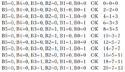
Figure 23: Execution result of the prime number DAC decoder verification program.
Remark 2
According to the Goldbach conjecture, any even number is the sum of two prime numbers. However, notice that its expression is not unique; a given even number n can be represented by and where are prime numbers. For example, in case n=18, 18=5+13 and 18=7+11. For the decoder design, we choose one of them for a given input data.
Dynamic element matching (DEM) techniques
(i)The prime number DAC has two current sources and in actual circuit, they can have mismatches ΔI as shown in Figure. 24 (a). However, using the pseudo-random switching, the mismatches can be time-averaged and the spurious components due to them can be spread out in frequency domain using simple circuitry as shown Figure. 24 (b).
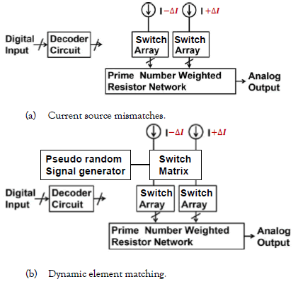
Figure 24: Current source mismatches and the prime number DAC with dynamic element matching circuit
(ii) Also the resistors can have mismatches as shown in Figure. 25. However, as the above “Remark 2” says, for a given input data, there can be multiple expressions of two-prime number sum. Suppose that the input is DC and its value is 9, and at time n, 9x2=5+13 is used while at time n+1, 9x2=7+11 is used. If such selections are done dynamically in a pseudo-random manner with modified decoder design, the resistor mismatch effects may be time-averaged and also the spurious components due to them may be spread out in frequency domain.
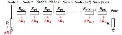
Figure 25: Resistor mismatches in the prime number DAC.
Application of these DEM techniques to the prime number DACs and also the N-polygonal number DACs should be further investigated as the next step.
Conclusion
This paper has demonstrated that new DAC architectures can be derived, based on number theory by integrating the knowledge of mathematics and physical electricity, and their operations are verified by simulation; the theoretical conjecture is consistent with the simulation results. Integers have very interesting properties, but they have not been fully exploited yet for the mixed-signal system and circuit design. We conclude this paper by remarking that in most cases, mixed-signal architecture design is based on designer’s experiences but not mathematics, and the attempt of its new architecture derivation from mathematics may have possibilities to lead to very new ones. As the next step, we will consider the derivation of the DAC architectures considering their practical aspects.
Acknowledgments
This work was supported by JSPS KAKENHI Grant Number 21K04190.
References
- Manganaro G, Advanced Data Converters. Camb. Univ. Press (2011).
- Maloberti F. Data Converters. Springer 2007;47-76.
- Plassche R , CMOS Integrated Analog-to-Digital and Digital-to-Analog Converters. Springer 2003.
- The Data Conversion Handbook. Analog Devices Inc. 2005.
- Dimopoulos H. Analog electronic filters: theory, design, and synthesis. Springer. 2011.
- Dickson M. History of the theory of numbers. Diophantine Analysis. Dover.2005;2.
- Kobayashi H, Aoki H, Katoh K, et al. Analog/Mixed-Signal circuit design in Nano CMOS Era.IEICE Electron Express. 2014;11(3): 20142001.
- Kobayashi H, Aoki H, Katoh K, et al. Analog/Mixed-Signal Circuit Testing Technologies in IoT Era. IEEE ICSICT.2020.
- Kobayashi H, Kushita N, Tran M, et al. Analog/Mixed-Signal/RF Circuits for Complex Signal Processing. IEEE ASICON. 2019.
- Kobayashi H, Machida K, Sasaki Y, et al. Fine Time Resolution TDC Architectures-Integral and Delta-Sigma Types. IEEE ASICON. 2019:1-4.
- Kobayashi H, Lin H. Analog/Mixed-Signal Circuit Design Based on Mathematics. IEEE ICSCIT.2016;930-33.
- Kobayashi H, Wei J, Murakami M. Performance Improvement of Delta-Sigma ADC/DAC/TDC Using Digital Technique. IEEE ICSICT. 2018;1-4.
- Kobayashi H, Sasaki Y, Arai H, et al. Unified Methodology of Analog/Mixed-Signal IC Design Based on Number Theory.IEEE ICSICT. 2018;1-4.
- Kobayashi Y, Kobayashi H. Redundant SAR ADC Algorithm Based on Fibonacci Sequence. Adv Micro-Device Eng Ⅵ Key Eng Mater. 2016; 698: 117-26.
- Yamamoto S, Sasaki Y, Zhao Y, et al. Metallic Ratio Equivalent-Time Sampling and Application to TDC Linearity Calibration. IEEE Trans Device Mater Reliab. 2022.
- Yamamoto S, Sasaki Y, Zhao Y, et al. Metallic ratio equivalent-time sampling: A highly efficient waveform acquisition method. IEEE IOLTS. 2021:1-6.
- Sasaki Y, Zhao Y, Kuwana A, et al. Highly efficient waveform acquisition condition in equivalent-time sampling system. IEEE Asian Test Symp. 2018:197-202.
- Katayama S, Abe Y, Kuwana A et al. Application of Residue Sampling to RF/AMS Device Testing. 30th IEEE Asian Test Symp. 2021:19-24.
- Abe Y, Katayama S, Li C, et al. Frequency Estimation Sampling Circuit Using Analog Hilbert Filter and Residue Number System. 13th IEEE Int Conf ASIC. 2019:1-4.
- Zhao Y, Katoh K, Kuwana A, et al. Revisit to histogram method for adc linearity test: Examination of input signal and ratio of input and sampling frequencies. J Electron Test: Theory Appl. 2022;38(1):21-38.
- Hirai M, Tanimoto H, Gendai Y, et al. Digital-to-analog converter configuration based on non-uniform current division resistive-ladder. ITC-CSCC. 2021:1-4.
- Hirai M, Tanimoto H, Gendai Y, et al. Nonlinearity Analysis of Resistive Ladder-Based Current-Steering Digital-to-Analog Converter. IEEE ISOCC. 2020:9-10
- Hirai M, Yamamoto S, Arai H, et al. Systematic Construction of Resistor Ladder Network for N-ary DACs. IEEE ASICON. 2019:1-4.
- Jiang R, Adhikari G, Sun Y, et al. Gray-code Input DAC Architecture for Clean Signal Generation. IEEE ISPACS. 2017:669-74.
- Adhikari G, Jiang R, Kobayashi H. Study of Gray Code Input DAC Using MOSFETs for Glitch Reduction. IEEE ICSICT. 2016:97-9.
- D. Yao A, Kuwana H, Kobayashi K, et al. Digital-to-Analog Converter Linearity Improvement Technique Based on Classical Number Theory for Modern ULSI. Int Workshop Post-Bin ULSI Syst. 2021.
- Higashino M, Mohyar S, Sun Y, et al. Digital-to-Analog Converter Layout Technique and Unit Cell Sorting Algorithm for Linearity Improvement Based on Magic Square. J Technol Soc Sci. 2020;4(1):22-35.
- Yao D, Sun Y, Higashino M, et al. DAC Linearity Improvement with Layout Technique using Magic and Latin Squares.IEEE ISPACS. 2017;616-21.
- Yao D, Bai x, Kuwana A, et al. Segmented DAC Unit Cell Selection Algorithm and Layout/Routing Based on Euler's Knight Tour. Int Conf Analog VLSI Circuits.2021.
- Du Y, Bai X, Hirai M, et al. Digital-to-Analog Converter Architectures Based on Polygonal and Prime Numbers.IEEE ISOCC. 2020;7-8.
- Du Y, Bai X, Hirai M, et al. Digital-to-Analog Converter Architectures Based on Goldbach Conjecture for Prime Numbers in Mixed-Signal ULSI.Int Workshop Post-Bin ULSI Syst. 2021.
- Du Y, Bai X, Tran M, et al. Design of Digital-to-Analog Converter Architectures Based on Polygonal Numbers. Int Conf Analog VLSI Circuits. 2021.