

Solder joints in surface mounted IC assemblies: Relief in stress and warpage owing to the application of elevated stand-off heights
2 Technical University, Vienna, Austria, and ERS Co., USA, Email: suhire@aol.com
Received: 12-Jan-2018 Accepted Date: Feb 12, 2018; Published: 19-Feb-2018
Citation: E. Suhir. Solder joints in surface mounted IC assemblies: Relief in stress and warpage owing to the application of elevated stand-off heights. J Mod Appl Phys. 2018;2(1):4-9.
This open-access article is distributed under the terms of the Creative Commons Attribution Non-Commercial License (CC BY-NC) (http://creativecommons.org/licenses/by-nc/4.0/), which permits reuse, distribution and reproduction of the article, provided that the original work is properly cited and the reuse is restricted to noncommercial purposes. For commercial reuse, contact reprints@pulsus.com
Abstract
The head-in-pillow (HnP) defects in Ball-Grid-Array (BGA) packages with leadfree solders and particularly in packages with fine ball pitches are attributed by the numerous investigators to three major causes: manufacturing process, solder material properties and design-related issues. The latter are thought to be caused mostly by warpage of the PCB-package assembly. In this analysis the warpage issue is addressed using an analytical predictive stress model. It is assumed that it is the difference in the post-fabrication deflections of the warped package and its PCB that are the root cause of the observed HnP defects. The calculated data suggest that the replacement of the conventional BGA design with a design with elevated stand-off heights of the solder joints, such as, eg, column-grid-array (CGA), could reduce the product’s propensity to warpage-related HnP defects. It is shown that, owing to the greater longitudinal interfacial compliance of the system employing solder joint interconnections with elevated standoff heights, significant stress relief and considerable decrease in the relative PCB vs. package warpage can be expected. In the carried out numerical example the effective stress in the solder material is relieved by about 40% and the difference between the maximum deflections of the PCB and the package is reduced by about 60%, when the conventional BGA design is replaced by the CGA system. There is a reason to believe that the application of BGA joints with CGA designs could result in a substantial improvement in the IC product’s reliability, including the it’s propensity to possible HnP defects. The stress model used in this analysis is a modification and extension of the model developed by the author back in mid-eighties. These models shed light on the underlying materials physics of the solder joint interconnections in surface mounted devices.
Keywords
Head-in-pillow; Column-grid-array; Interfacial shearing stress; Solder joints; Stress
Introduction
The causes of the observed head-in-pillow (HnP) soldering defects in BGA packages with lead-free solders [1-9] are attributed to various processrelated, solder-material-related and design-related issues. The design-related problems are caused by the elevated warpage of the PCB-package assembly. Because of that, in some IC package designs package structures of the type shown in Figure 1 are used. Such structures are, however, too expensive, and it is more often than not that no metal frames are used in the to-days package technologies. A typical today’s IC package structure (Figure 2) and is addressed in our analysis. The emphasis on the warpage issue. It is assumed that it is the difference in the post-fabrication thermally induced deflections of the warped PCB and the also warped package that is the root cause of the possible HnP defects, as well as, of course, in an insufficient interfacial strength of the solder joint interconnections. The advantages of the elevated stand-off heights of solder joint interconnections have been first indicated in application to flip-chip solder joints [10,11] (Figures 3 and 4), i.e., to the s.c. first level of interconnections, and is recently addressed in application to the second level of interconnections [12], including CGA designs [13-19] (Figure 5).

Figure 1: SMT package with a metal frame to prevent post-fabrication warpage

Figure 2: Typical today’s SMT package surface-mounted on a PCB

Figure 3: Solder joint modeled as a short circular cylinder (“column”) clamped at its end planes and experiencing axisymmetric elastic deformation caused by the local thermal mismatch of the solder material with the Si material of the substrates. The induced maximum stresses and strains are in the vertical direction, while the external mismatch strains act in the horizontal planes

Figure 4: Solder joints configured as short cylinders experience much lower stresses and strains than those configured as “pancakes”

Figure 5: BGA vs. CGA designs
Analysis
Interfacial shearing stress
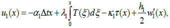
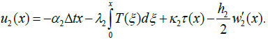
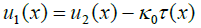
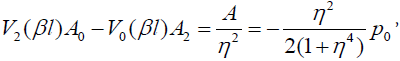
Let a BGA or a CGA assembly be fabricated at an elevated temperature and subsequently cooled down to a low (room or testing) temperature. The interfacial longitudinal displacements and in the PCB (component #1) and in the package (component #2) BGA- or CGA- bonded on the PCB can be sought, in an approximate analysis, based on the concept of the interfacial compliance [19] as follows:
 (1)
(1)
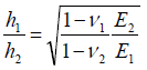
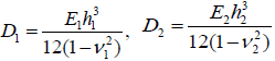
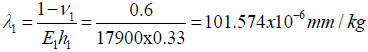
Here Δt is the change in temperature, α1 and α2 are the effective CTEs of the component materials (these should be assessed, in an approximate fashion, for the composite structures of the PCB and package), h1 and h2 are their thicknesses,
 and
and
 are the axial compliances of the components, E1 and E2 are the effective Young’s moluli of the
component materials (assessed, in an approximate fashion, for the composite structures of the PCB and package), ν1 and ν2 are their Poisson’s ratios,
are the axial compliances of the components, E1 and E2 are the effective Young’s moluli of the
component materials (assessed, in an approximate fashion, for the composite structures of the PCB and package), ν1 and ν2 are their Poisson’s ratios,
 and
and
 are the longitudinal interfacial compliances of the components,
 and
and
 are shear moduli of their materials,
 (2)
(2)
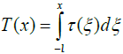
are the forces acting in the cross-sections of the assembly components(tensile - in the PCB and compressive - in the package), τ(x) is the interfacial shearing stress, l is half the assembly length, and w1(x) w2(x) are the deflections of the PCB and package. The origin of the longitudinal coordinate x is in mid-cross-section of the assembly.
The first terms in the equations (1) are unrestricted (stress-free) displacements. The second terms are displacements caused by the thermally induced forces acting in the cross-sections of the assembly components. Hooke’s law is used to structure these terms, assuming that the displacements of all the points of the given cross-section are the same. The third terms are, in effect, corrections to such an assumption. They consider that the longitudinal displacements of the points at the interface are somewhat larger than the displacements of the inner points of the given cross-section. It is assumed that this correction can be sought as a product of the known interfacial compliance of the component and the thus far unknown interfacial shearing stress. The last terms in (1) are due to bending.
The condition
 (3)
(3)
of the compatibility of the displacements (1) considers that these displacements differ, because of the interfacial compliance
 (4)
(4)
of the bonding (solder) layer, by the amount expressed by the second term in the right part of the condition (3). In the formula (4),
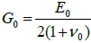 is the
shear modulus of the bonding material (solder joint system), E0 is its Young’s
modulus, and ν0 is its Poisson’s ratio. Introducing the expressions (1) for the
longitudinal interfacial displacements into the condition (3), the following
equation for the interfacial shearing stress τ(x) can be obtained:
is the
shear modulus of the bonding material (solder joint system), E0 is its Young’s
modulus, and ν0 is its Poisson’s ratio. Introducing the expressions (1) for the
longitudinal interfacial displacements into the condition (3), the following
equation for the interfacial shearing stress τ(x) can be obtained:
 (5)
(5)
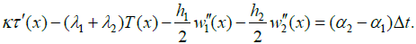
Here K = K0 + K1 + K2 is the total longitudinal interfacial compliance of the assembly. By differentiation we find:
 (6)
(6)
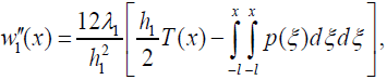
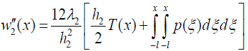
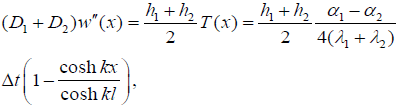
Assuming that the assembly components can be treated as thin rectangular plates and that their curvatures in the x and y directions at the given point of the assembly are equal, the equations of bending of the PCB (component #1) and the package (component #2) can be written as
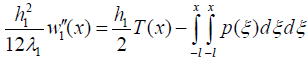
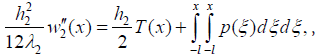 (7)
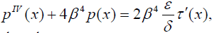
(7)
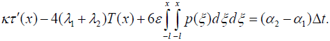
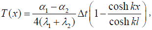
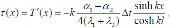
where p(x) is the interfacial peeling stress. The left parts of these equations are the elastic bending moments. The first terms at the right parts are bending moments caused by the thermal forces T(x). The second terms are the bending moments caused by the peeling stress p(x). Introducing the formulas
 (8)
(8)
for the curvatures into the equation (6), the following relationship can be obtained:
 (9)
(9)
Here the notation
 (10)
(10)
is used. The formula (10) indicates particularly that the role of the peeling stress can be minimized if the relationship
 (11)
(11)
is fulfilled. This circumstance might have a favorable effect on the HnP design-related problem.
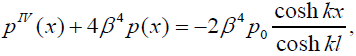
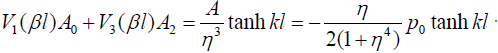
In an approximate analysis below we assume that the peeling stress need not be considered when the interfacial shearing stress is evaluated, i.e. does not affect the interfacial shearing stress. Then the latter can be determined from the simplified equation
 (12)
(12)
At the end of the assembly the boundary condition T(l) = 0 should be fulfilled. Then the equation (12) results in the following boundary condition for the shearing stress function
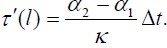 (13)
(13)
The force T(x) should be symmetric with respect to the mid-cross-section of the assembly, and could be sought therefore as
 (14)
(14)
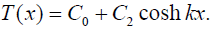
Here C0 and C2 are constants of integration, and k is thus far unknown parameter of the interfacial shearing stress. As follows from (2), the interfacial shearing stress τ(x) is related to the thermal force T(x) as follows:
 (15)
(15)
Introducing the expressions (14) and (15) into the equation (12), one concludes that this equation is fulfilled if the following relationships take place:
 (16)
(16)
The second formula in (16) determines the parameter of the interfacial shearing stress. Note that this parameter is independent from the external strain (α1 - α2)Δt and is a characteristic of the structure, and not the loading.
From (15) we obtain:
 (17)
(17)
The boundary condition (13), considering the second formula in (16), yields:
 (18)
(18)
and the solutions (14) and (15) result in the following expressions for the forces T(x) acting in the components’ cross-sections and the interfacial shearing stress τ(x):
 (19)
(19)
Interfacial peeling stress
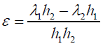
It is natural to assume that the peeling stress p(x) in the given crosssection is proportional to the difference in the deflections of the assembly components in this cross-section:
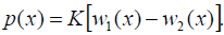 (20)
(20)
It is this stress that is thought to be responsible for the possible occurrence of the HnP defects. The stiffness K in this formula can be assessed, using an analogy with the longitudinal interfacial compliances, by the formula
 (21)
(21)
Differentiating the relationship (20) twice, we obtain:
 (22)
(22)
Introducing the formulas (8) into this equation and differentiating the obtained relationship twice, the following equation for the peeling stress can be obtained:
 (23)
(23)
where the notations
 (24)
(24)
are used. The right part of the equation (23) indicates that the longitudinal gradient of the interfacial stress plays the role of the excitation force for the peeling stress.
Considering the second formula in (19), the equation (23) yields:
 (25)
(25)
where the notation
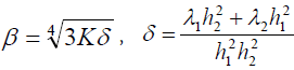
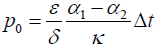 (26)
(26)
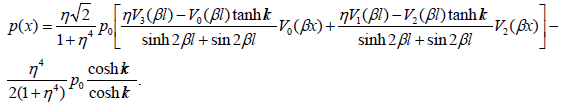
is used. It will be shown below that this peeling stress is twice as high as the peeling stress at the end of a long-and-stiff assembly.
The solution to the equation (25) can be sought in the form:
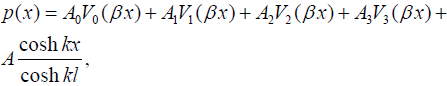 (27)
(27)
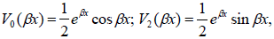
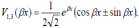
where the functions Vi(βx),i=0,1, 2,3,

 (28)
(28)
obey the following simple and convenient rules of differentiation:

 (29)
(29)
Introducing the sought solution (27) into the equation (25), we obtain:
 (30)
(30)
where the notation
 (31)
(31)
is used.
There are neither concentrated bending moments, nor lateral forces acting at the assembly ends, and therefore the boundary conditions
 (32)
(32)
for the deflection functions w1(x) and w2(x) should take place. Using the formula (20) these conditions yield:
 (33)
(33)
The peeling stress should be symmetric with respect to the mid-cross-section of the assembly, and therefore the coefficients in front of the odd functions in the solution (27) can be put equal to zero. Then the peeling stress can be sought in the form
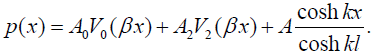 (34)
(34)
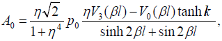
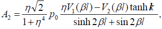
The conditions (33) result in the following equations for the constants A0 and A2 of integration:
 (35)
(35)
These equations have the following solutions:
 (36)
(36)
and the solution (34) yields:
 (37)
(37)
For long-and-stiff enough assemblies, typical in the designs of interest,
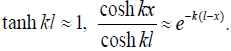 (38)
(38)
Then the solution (37) can be simplified:
 (39)
(39)
At the assembly ends (x = l)
 (40)
(40)
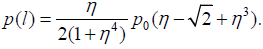
If the assembly is very stiff in the through-thickness direction, i.e. characterized by large η values, then the formula (40) yields:
 . This result explains the physical meaning of the p0 value, introduced by the
notation (26): it is the stress that is twice as high as the peeling stress at the
end of a very long-and-stiff assembly. When the ratio η changes from zero
to infinity, the stress p(l) changes from zero to
. This result explains the physical meaning of the p0 value, introduced by the
notation (26): it is the stress that is twice as high as the peeling stress at the
end of a very long-and-stiff assembly. When the ratio η changes from zero
to infinity, the stress p(l) changes from zero to
 . As has been shown
above, the p0 value can be made low, if the relationship (11) is fulfilled.
Warpage
. As has been shown
above, the p0 value can be made low, if the relationship (11) is fulfilled.
Warpage
The bow of the assembly as a whole can be determined from the equation
 (41)
(41)
where
 (42)
(42)
are the flexural rigidities of the assembly components. From (41) the following formula for the assembly curvature can be obtained:
 (43)
(43)
where
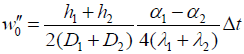 (44)
(44)
is the curvature in the middle of a long-and-stiff assembly. As evident from the expression (43), the assembly curvature changes from its maximum value
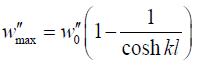 (45)
(45)
in the middle of the assembly to zero at its ends. From (43) we find the following expression for the angles of rotation:
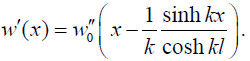 (46)
(46)
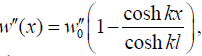
Assuming that the assembly ends have zero deflection, this expression results in the following formula for the assembly deflections:
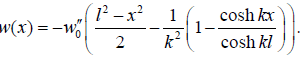 (47)
(47)
In the middle of the assembly (x = 0)
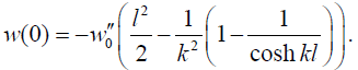 (48)
(48)
In the case of a long and/or stiff assembly (large kl values),
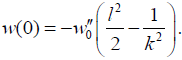 (49)
(49)
For assemblies having very high k values (stiff PCB, stiff package, and stiff solder system) this formula yields:
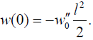 (50)
(50)
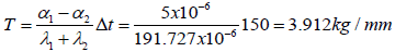
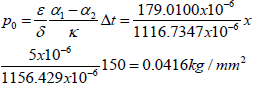
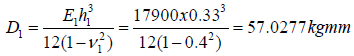
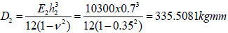
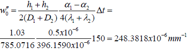
The assembly size (half-length) is l= 20.0mm, and the change in temperature is Δt =150°C.
Computed data:
Axial compliances:
Numerical Example
| Structural element | PCB | Package | BGA | CGA |
|---|---|---|---|---|
| Element # | 1 | 2 | 0 | 0 |
| CTE (1/°C) | 15 x10-6 | 10 x 10-6 | x | x |
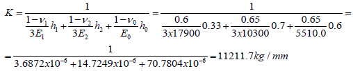
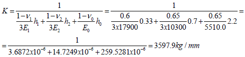
| Young’s Modulus (E,Kg/mm2) | 17900 | 10300 | 5510 | 5510 |
| Poisson’s ratio (V) | 0.4 | 0.35 | 0.35 | 0.35 |
| Thickness/height (h,mm) | 0.33 | 0.7 | 0.6 | 2.2 |
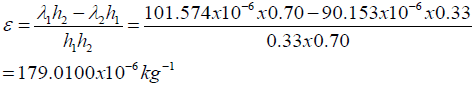
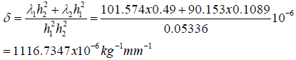
| Shear modulus (G,Kg/mm) | 6393 | 3815 | 2040.7 | 2040.7 |
| Axial compliance (λ mm/Kg) | 101.574 x 10⁻⁶ | 90.153 x 10⁻⁶ | x | x |
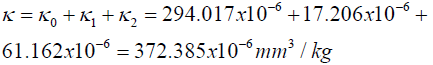
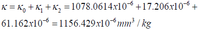
| Interfacial compliance (K, mm3/Kg) | 17.206x10⁻⁶ | 61.162x10⁻⁶ | 294.017x10⁻⁶ | 1078.061x10-6 |
PCB:
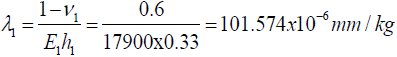
Package:

Interfacial compliances:
PCB:

Package:
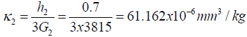
BGA system:
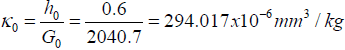
CGA system:
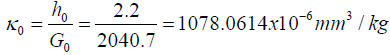
Total interfacial compliance:
with the BGA system:
with CGA system:
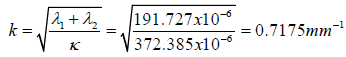
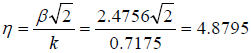
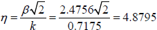
Parameter of the interfacial shearing stress:
with the BGA system:
with the CGA system:
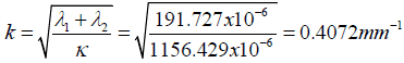
Product kl is kl = 0.7175x20 =14.350 for the BGA design and is kl = 0.4072x20 = 8.1440 for the CGA design. In either case it is significant, so that the assembly can be treated as a long one.
Thermal force in the mid-cross-sections of the assembly:
Maximum interfacial shearing stress (at the assembly ends):
with the BGA system:

with the CGA system:

Axial compliance related parameters:
The doubled interfacial peeling stress at the end of a stiff assembly
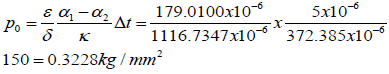
in the case of the BGA solder and is
in the case of the CGA solder.
The interfacial through-thickness spring constant is
with the BGA solders and
with the CGA solders.
Parameter of the peeling stress

in the case of the BGA system and

in the case of the CGA design.
The ratio of the parameters of the interfacial peeling and the shearing stresses
in the case of a BGA and is
in the case of a CGA.
The peeling stress at the assembly end is
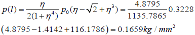
in the case of the BGA system and is
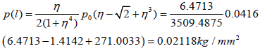
when the CGA system is employed.
The effective stress is
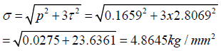
in the case of a BGA and is
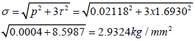
in the case of a CGA design.
Flexural rigidities of the PCB and the package:
Curvature in the middle of a long-and-stiff assembly:
Maximum bow:
with the BGA assembly:
with the CGA assembly:
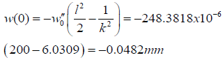
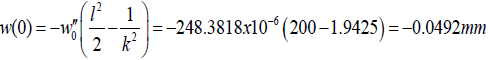
The difference in maximum deflections
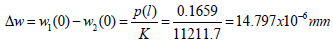
in the BGA design and
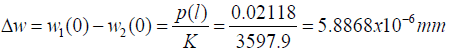
in the CGA design (Table 1).
Table 1: The calculated data are summarized in the following table
| Stress and bow | Shearing stress (Kg/mm2) | Peeling stress (Kg/mm2) | Effective stress(Kg/mm2) | Maximum bow, mm | Mm Δw= w1-w2 mm |
|---|---|---|---|---|---|
| BGA | 2.8069 | 0.1659 | 4.8645 | -0.0492 | 1.48E-05 |
| CGA | 1.693 | 0.02118 | 2.937 | -0.0482 | 5.89E-06 |
These data indicate that the application of the CGA technology, instead of the BGA design can result in significant stress relief and, hence, in a high likelihood that the warpage-related HnP defects could be minimized or even avoided.
Conclusion
The application of the CGA technology, instead of the BGA design, can result in significant stress relief and, supposedly, in a high likelihood that the warpage-related HnP defects could be minimized or even avoided. Future work should include FEA and experimental investigations.
REFERENCES
- Bath J, Garcia R, Christopher A, et al. Plastic ball grid array package warpage and impact on traditional MSL classification for Pb free assembly SMTAI Conference. 2004.
- Lathrop L. BGA Co-planarity reduction during the ball attaches process, SMTAI pan pacific conference. 2008
- Tsai MY, Hsu CH, Han CN. A note on suhir’s solution of thermal stresses for a die substrate assembly. ASME J Electronic Packaging. 2004: 126.
- Tsai MY, Hsu CH, Wang CT. Investigation of thermo mechanical behaviors of Flip-Chip BGA Package during manufacturing process and thermal cycling, IEEE CPMT Transactions. 2004; 27.
- Dudi A, Aspandiar R, Buttars S, et al. head on pillow SMT failure modes SMTAI Conference. 2009.
- Savic J, Xie W, Islam N, et al. Warpage mitigation processes in the assembly of large body size mixed pitch BGA coreless packages for use in high speed network applications SMTAI Conference. 2013.
- Liu Y, Fiacco P, Lee N. Testing and prevention of head in pillow ECTC. 2010.
- High temperature printed board flattness guideline IPC. 2013.
- Rekers H, Eng P. Case study head in pillow defect on a plastic BGA, SMTAI Conference on soldering and reliability. 2015;10.
- Suhir E. Axisymmetric elastic deformations of a finite circular cylinder with application to low temperature strains and stresses in solder Joints. ASME J Appl Mech.1989;56.
- Suhir E. Mechanical reliability of flip-chip interconnections in silicon-on-silicon multichip modules, IEEE Conference Santa Cruz California March 1993.
- Suhir E. Analysis of a short beam with application to solder joints could larger stand-off heights relieve stress, (EPJAP), 2015: 71.
- Suhir E. Predicted Stresses in a ball grid array (BGA)/column-grid-array (CGA) assembly with a low modulus solder at its ends. J Mat Science, Materials in Electronics.2015;26.
- Suhir E, Ghaffarian R, Nicolics J. Could application of column-grid array technology result in inelastic strain free state of stress in solder Material, J Mat Sci, Materials in Electronics. 2015;26.
- Suhir E, Ghaffarian R, Nicolics J. Could thermal stresses in an inhomogeneous BGA/CGA System be predicted using a model for a homogeneously bonded assembly. J Mat Sci, Materials in Electronics 2016: 27.
- Suhir E, Ghaffarian R, Nicolics J. Predicted stresses in ball grid array (BGA) and column-grid-array (CGA) interconnections in a mirror like package design, J Mat Sci Materials in Electronics. 2016;27.
- Suhir E, Ghaffarian R. Predicted stresses in a ball grid-array (BGA)/column-grid-array (CGA) assembly with epoxy adhesive at its ends, J Mat Sci, Materials in Electronics. 2016;27.
- Suhir E, Ghaffarian R. Column grid array (CGA) vs ball grid-array (BGA) board-level drop test and the expected dynamic stress in the solder material, J Mat Sci, Materials in Electronics. 2016;27.
- Suhir E. Die attachment design and its influence on thermal stresses in the die and the attachment, ECTC. 1987